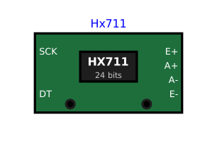
modelHx711

Extends from Internal.Devices.PartialSupplyPin (Supply of a peripheral: optional GND and VCC pins, internal supply rail - GND shown and ideal internal supply VOH by default).
Information
The HX711 (Avia Semiconductor) is the converter of electronic scales: a programmable-gain amplifier followed by a 24-bit analog-to-digital converter, designed to read a gauge bridge directly. This model reproduces its behaviour as seen from the microcontroller, based on the datasheet.
Bridge side
The module supplies the bridge through E+/E− (voltage AVDD) and measures the differential voltage between A+ and A−. The conversion is ratiometric: the result depends on the ratio between the bridge output and its excitation, not on the value of the supply.
code = vIn · gain / vRef · 224, rounded and clamped to [−223, 223−1] (full scale: ±AVDD/(2·gain), i.e. ±17 mV at gain 128).
Microcontroller side
- Every
1/rateseconds, a new data is ready:DOUTgoes to 0. If the previous one has not been read,DOUTfirst goes back up briefly (tUpdate), so that each new data is announced by a falling edge. - Each rising edge of
PD_SCKshifts a bit out onDOUT, most significant first. After the 24 data bits, 1 to 3 extra pulses choose the gain of the next conversion: 25 pulses → 128 (channel A), 26 → 32 (channel B), 27 → 64 (channel A).DOUTthen goes back to 1. PD_SCKheld high for more than 60 µs powers the chip down. When it returns to 0, the chip restarts as at power-up: gain 128, and first data after 4 conversions (400 ms at 10 samples/s).
The microcontroller therefore drives PD_SCK bit by bit (bit-banging). Its pin accesses must take simulated time (parameter MCU.gpioOpTime, 5 µs by default): otherwise, the pulses would have a zero duration.
Simplifications
- Channel B (inputs B+/B−, gain 32) is not wired: it reads 0 V.
- Each conversion is an instantaneous sample of the input (no averaging over the period), with no settling time after a gain change.
- The noise (
noiseLsb, standard deviation in LSB) is Gaussian and reproducible: theseedfixes the sequence of draws.
The icon shows the gain and the last converted code. The cyan light signals a data ready, the amber light the power-down.
Parameters
| Type | Name | Default | Description |
|---|---|---|---|
| Electrical › Supply | |||
| Boolean | useSupplyPin (from PartialSupplyPin) | false | Show the VCC supply pin: the peripheral is supplied by the circuit (its high levels follow VCC, its consumption IQ is drawn from VCC) - unchecked: ideal internal supply VOH, nothing to wire |
| Modelica.Units.SI.Voltage | VOH (from PartialSupplyPin) | Interfaces.VOH | Logic high voltage: ideal internal supply, high level of the outputs and of the pull-ups - with the VCC pin, the voltage of VCC is used instead |
| Modelica.Units.SI.Current | IQ (from PartialSupplyPin) | 1e-3 | Current drawn from VCC by the peripheral (quiescent consumption, outputs excluded) |
| Boolean | useGroundPin (from PartialSupplyPin) | true | Show the GND pin - unchecked: the peripheral is referenced to the simulation ground (0 V), nothing to wire |
| SI.Voltage | VDropout | 0.1 | Dropout of the analog regulator of the module: with the VCC pin, AVDD is limited to VCC - VDropout |
| Conversion | |||
| Real | rate | 10 | Conversion rate (RATE pin of the chip: 10 or 80 samples per second) |
| SI.Voltage | AVDD | 4.3 | Excitation voltage of the bridge, E+ output (module supplied with 5 V) - with the VCC pin, at most VCC - VDropout |
| Real | noiseLsb | 0 | Conversion noise, standard deviation in LSB (0 = perfect, reproducible measurement) |
| Integer | seed | 711 | Noise seed: same seed, same sequence of measurements |
| Timing | |||
| SI.Time | tPowerDown | 60e-6 | PD_SCK held high longer than this: power-down |
| SI.Time | tUpdate | 10e-6 | Time during which DOUT goes back up before each new data, when the previous one has not been read |
| Integer | settlingConversions | 4 | Conversions discarded after power-up or wake-up (400 ms at 10 samples/s) |
| Electrical › Levels | |||
| SI.Voltage | VOL | Interfaces.VOL | Low level of DOUT |
| SI.Voltage | VIH | Interfaces.VIH | Threshold above which an input reads high (PD_SCK) |
| SI.Voltage | VIL | Interfaces.VIL | Threshold below which an input reads low (PD_SCK) |
| Electrical › Impedances | |||
| SI.Resistance | ROut | Interfaces.ROut | Series resistance of the DOUT output |
Connectors
| Type | Name | Default | Description |
|---|---|---|---|
| Modelica.Electrical.Analog.Interfaces.NegativePin | GND (from PartialSupplyPin) | Common reference (ground), to be connected to the microcontroller's one - shown when useGroundPin is checked | |
| Modelica.Electrical.Analog.Interfaces.PositivePin | VCC (from PartialSupplyPin) | Supply of the peripheral (e.g. 3V3(OUT) of a Raspberry Pi Pico) - shown when useSupplyPin is checked | |
| Modelica.Electrical.Analog.Interfaces.PositivePin | PD_SCK | Serial clock and power-down control (SCK pin of the module), driven by the microcontroller | |
| Modelica.Electrical.Analog.Interfaces.PositivePin | DOUT | Serial data (DT pin of the module), read by the microcontroller | |
| Modelica.Electrical.Analog.Interfaces.PositivePin | E_plus | Bridge excitation (+) | |
| Modelica.Electrical.Analog.Interfaces.PositivePin | A_plus | Differential input of channel A (+), from S+ of the bridge | |
| Modelica.Electrical.Analog.Interfaces.NegativePin | A_minus | Differential input of channel A (-), from S- of the bridge | |
| Modelica.Electrical.Analog.Interfaces.NegativePin | E_minus | Bridge excitation (-), connected to the module ground |
Components
| Type | Name | Default | Description |
|---|---|---|---|
| Integer | code | Last conversion result (two's complement, 24 bits) | |
| Integer | gain | Gain of the current conversion (128 or 64 on channel A, 32 on channel B) | |
| Integer | pulses | PD_SCK pulses received since the data became ready | |
| Boolean | ready | Data ready, not read yet: DOUT is at 0 | |
| Boolean | poweredDown | Powered down (PD_SCK held high longer than tPowerDown) | |
| SI.Voltage | vIn | Differential voltage of channel A, A+ - A- | |
| SI.Voltage | vRef | Excitation voltage, E+ - E-: reference of the conversion (ratiometric measurement) |